
CPU, Nanometres and How Chips Are Actually Made
A chip sold as three nanometres has nothing on it that is three nanometres across. This video explains what the number in a chip's name really is, and how chips are actually made.
It starts with the first transistor at Bell Labs (16 December 1947), Kilby's first integrated circuit (12 September 1958) and Noyce's planar chip, then Moore's 1965 prediction and Dennard's 1974 scaling paper. From the Intel 4004 (15 November 1971, 2,300 transistors, a 10-micron process) to the late 1990s, a node's name was its gate length. Then the two came apart: by Intel's own account, nanometre naming stopped matching the gate length in 1997.
Then the factory: silicon purified to eleven nines, grown into a single-crystal ingot and sliced into 300 mm wafers; lithography, where up to 100 layers are printed with light through a mask; and ASML's extreme ultraviolet machines, which make 13.5 nm light by hitting tin droplets with lasers up to 50,000 times a second.
Every figure is on screen with its source and date. Vendor performance figures are the companies' own claims, shown against the baseline node they name.
In these topics
Chapters
Video notes
1. What does three nanometres measure?

Every phone, laptop and games console runs on chips packed with tiny switches. When a new chip is launched, it usually comes with a number attached, given in nanometres. A nanometre is a billionth of a metre, so the number sounds like a measurement of something very small.
That number is the name of a process node. A process node is a generation of manufacturing: the recipe a factory follows to make a chip, and the machines it uses to do it. Newer chips are made on newer nodes, and the newest carry names such as three nanometres, or two.
This video asks what that number actually measures. It starts with the first transistor, built in nineteen forty-seven. It follows the switches as they shrank, and finds the moment the name stopped matching them. Then it goes inside the factory, to the light that prints a modern chip. And it ends with the race to the next names, which have dropped nanometres altogether.
Here is the surprise, and it is one the industry openly admits. The number in the name no longer describes the size of any particular part of the chip.
Take the generation called five nanometres. In twenty twenty, the magazine IEEE Spectrum reported two of its key spacings, from a scheme proposed for the industry's own roadmap. The switches sat forty-eight nanometres apart. The finest wires joining them sat thirty-six nanometres apart.
Neither number is five. And the name itself does not say which part of the chip it is supposed to describe.
So the name is a label, a bit like a model year on a car. It still tells you something real, because a newer node fits more switches into the same area, and usually runs them faster or on less power. What it no longer tells you is the size of anything.
To see how the name came loose from the thing it named, the story has to start with the switch itself.
2. The switch
A computer chip is made of transistors. A transistor is a switch with no moving parts. A small voltage on one connection decides whether current can flow between the other two. On stands for one and off stands for zero, and every calculation a computer does is built out of those two states.
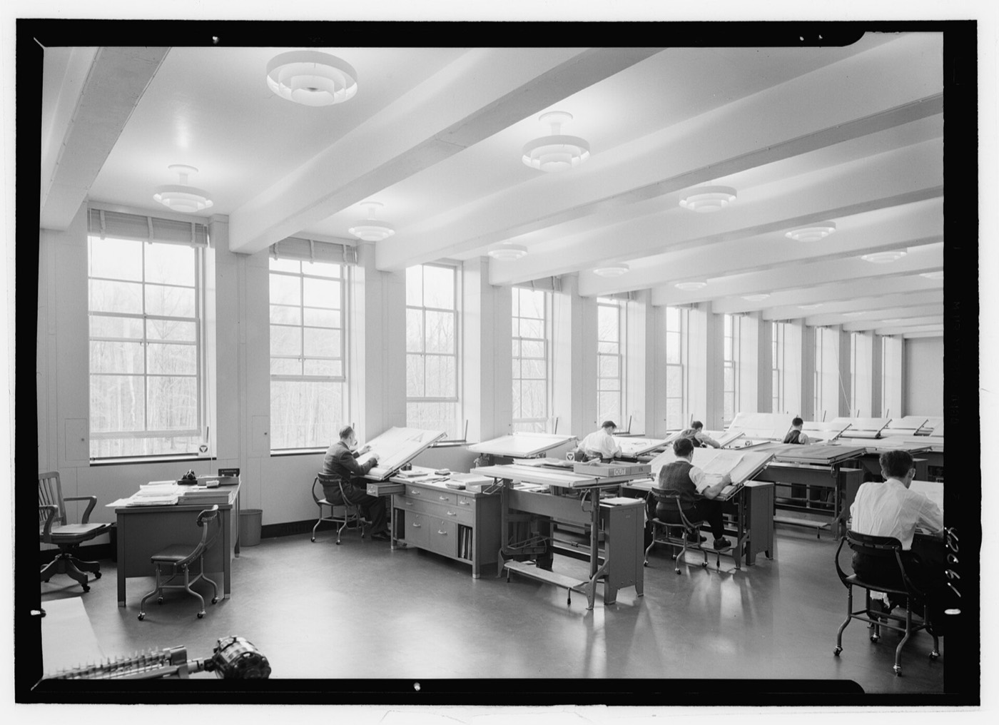
The first transistor was built at Bell Telephone Laboratories, the research arm of the Bell telephone company. Its main site was at Murray Hill, in New Jersey. This photograph of the laboratories was taken in the early nineteen forties, a few years before the breakthrough.
Before transistors, the switching in electronics was done by vacuum tubes. These were glass bulbs that glowed hot, used a lot of power and burned out. The telephone company wanted something smaller and more reliable, so it set a team of physicists to work on semiconductors.
A semiconductor is a material that sits between a conductor, which carries electricity freely, and an insulator, which blocks it. Germanium and silicon are the best known. Treat one the right way, and you can control whether it conducts, which is exactly what a switch needs.
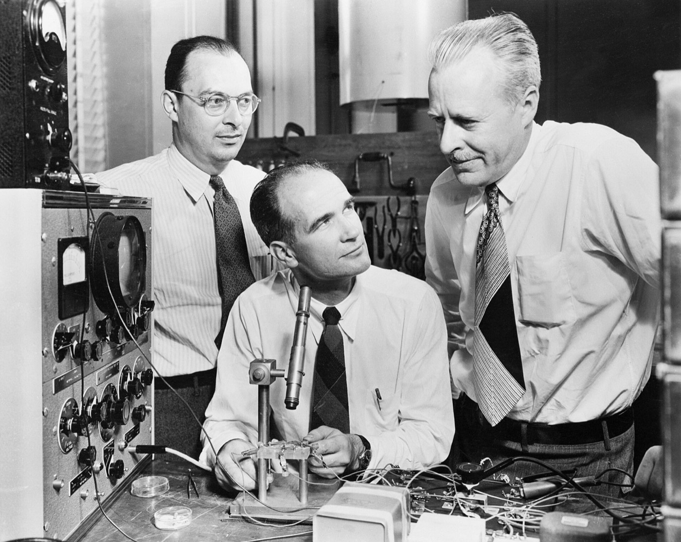
The team was led by William Shockley. Two of its members, John Bardeen and Walter Brattain, did the decisive experiment. This is the three of them, in a Bell Labs publicity photograph from nineteen forty-eight.
On the sixteenth of December, nineteen forty-seven, their device worked. A voltage on one contact controlled the current flowing through another. According to the Computer History Museum, it made the input signal up to a hundred times stronger.
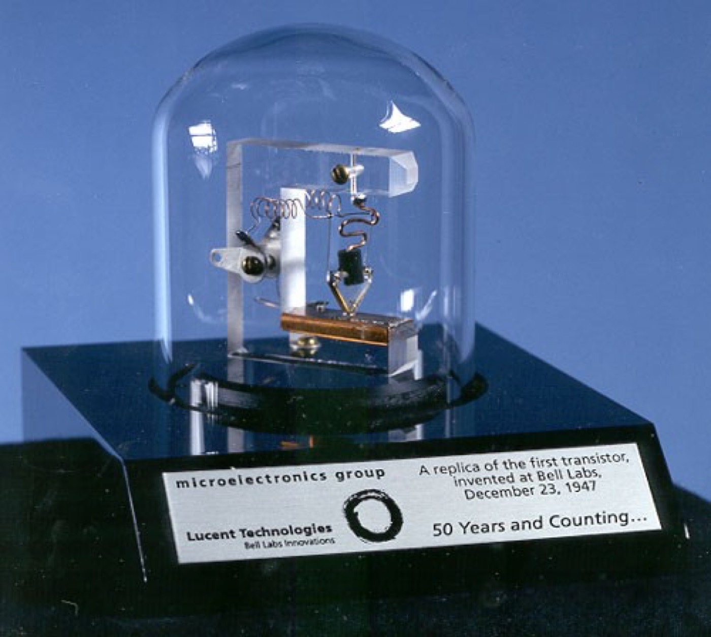
It was called a point-contact transistor. Two fine contacts pressed onto a small slab of high-purity germanium, and the signal passing between them could be controlled. This is a replica of that first device.
It proved the idea. What it could not do was scale, because every transistor had to be made and wired up on its own. The next step was to make many switches at once.
3. Many switches on one chip
By the late nineteen fifties, transistors were going into radios and computers. But each one was still a separate part, soldered to the next. A computer needed a great many of them, and every soldered joint was another chance for a fault.
The answer was the integrated circuit. That is a complete circuit, with its switches and the parts between them, made in one piece of semiconductor. Today it is usually just called a chip.
Two people got there within months of each other. Jack Kilby worked at Texas Instruments, in Dallas. Robert Noyce was at Fairchild Semiconductor, in what would become known as Silicon Valley, in California.
On the twelfth of September, nineteen fifty-eight, Kilby's first circuit worked. He had etched a transistor, a capacitor and a resistor into slices of germanium. But he joined those parts together with fine gold wires, one by one.
Noyce's version solved the wiring. It built on the planar process, worked out by his Fairchild colleague Jean Hoerni in nineteen fifty-nine, and planar simply means flat. The parts sat flat in the silicon under a protective layer of oxide, and thin metal lines laid on top joined them together.
Noyce filed his patent on the thirtieth of July, nineteen fifty-nine. It was granted in April nineteen sixty-one. In between, in May nineteen sixty, Fairchild's engineers made the first working chips of this kind. Kilby and Noyce are now credited together as co-inventors of the integrated circuit.
The planar method mattered more than any single chip. Because the parts and the wiring were laid down in flat layers, a whole circuit could be printed rather than assembled. And anything that can be printed can be made smaller, and made in large numbers.
4. Moore's bet

Printing chips raised an obvious question: how far could it go? In nineteen sixty-five, Fairchild's director of research and development, Gordon Moore, wrote an article about it for Electronics magazine.
The article appeared on the nineteenth of April, nineteen sixty-five. Moore looked at chips made from nineteen fifty-nine to nineteen sixty-four, and saw the number of parts on each one doubling every year. He projected that a single chip could hold sixty-five thousand parts by nineteen seventy-five.
That prediction became known as Moore's law. It is not a law of nature. It is an observation about an industry, and it became a yardstick the industry measured itself against.
In nineteen seventy-five, Moore revised his forecast. Chips for processors were less densely packed than memory chips, so he changed his estimate to a doubling every two years. That is the version usually quoted today.
Moore's law described what was happening. It did not explain why shrinking was so worth doing. That explanation came from IBM.
In October nineteen seventy-four, the IBM researcher Robert Dennard and his colleagues published a paper on scaling. It showed that when a transistor's dimensions were scaled down by some factor, its speed improved by that same factor. Shrinking the switch also cut the power it used.
So every step down was a win three times over. Smaller switches were faster, used less power, and more of them fitted on each chip. For decades after that paper, a new generation of chips meant exactly that.
5. When the name was a length
In those years, the name of each generation was a real measurement. It was the length of the gate.
The gate is the part of a transistor that switches it on and off. Current flows through a channel underneath it, from one side to the other. Gate length is how far that current travels under the gate, and the shorter it is, the faster the switch.
A microprocessor is a computer's central processing unit, its CPU, on a single chip. The first one shows what those gate lengths were like.
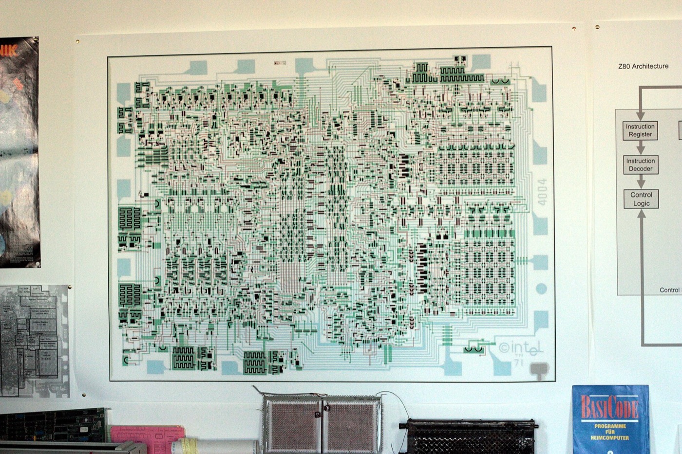
Intel's 4004 put a whole processor on one piece of silicon. This is its layout drawing, the plan of the patterns printed onto the chip, from nineteen seventy-one. Each shape stands for part of a layer.
Intel dates the 4004 to the fifteenth of November, nineteen seventy-one. It held twenty-three hundred transistors. They were made on a ten-micron process, and a micron is a thousand nanometres.
Until the late nineteen nineties, the name and the gate length moved together. Each generation shrank the gate and took its name from it. IEEE Spectrum gives the example of the point three five micron node, in the mid-nineteen nineties, whose name described its gate length.
Then the two came apart. The point two five micron node arrived in nineteen ninety-seven. According to a survey by Kevin Morris for the website EEJournal, its gate was two hundred nanometres long, shorter than the name. By the hundred and thirty nanometre node, the gate was just seventy.
For a while the name was modest, because the real gate was shorter than the name said. Then it swung the other way. Morris gives Intel's twenty-two nanometre node a gate twenty-six nanometres long. Its ten nanometre node had a gate of eighteen, so the names were now smaller than the things they seemed to describe.
His conclusion was blunt. Since nineteen ninety-seven, he wrote, "the node name has not been a representation of any actual dimension on the chip". The label had outlived the measurement.
6. Sand to wafer
So what is a modern chip actually made of, and how? It starts as silicon, the element found in ordinary sand and quartz.
The silicon has to be purified first. The Japanese chipmaker Rapidus describes the standard as eleven nines: ninety-nine point nine nine nine nine nine nine nine nine nine per cent pure. Put another way, that is no more than one stray atom in every hundred billion.
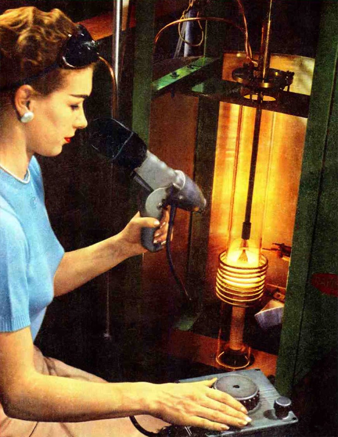
The pure silicon is melted in a quartz crucible, at about one thousand four hundred and twenty degrees Celsius. A small seed crystal is touched to the surface, then slowly pulled up and turned. This photograph from nineteen fifty-six shows the same method, called the Czochralski method, at a Raytheon plant.
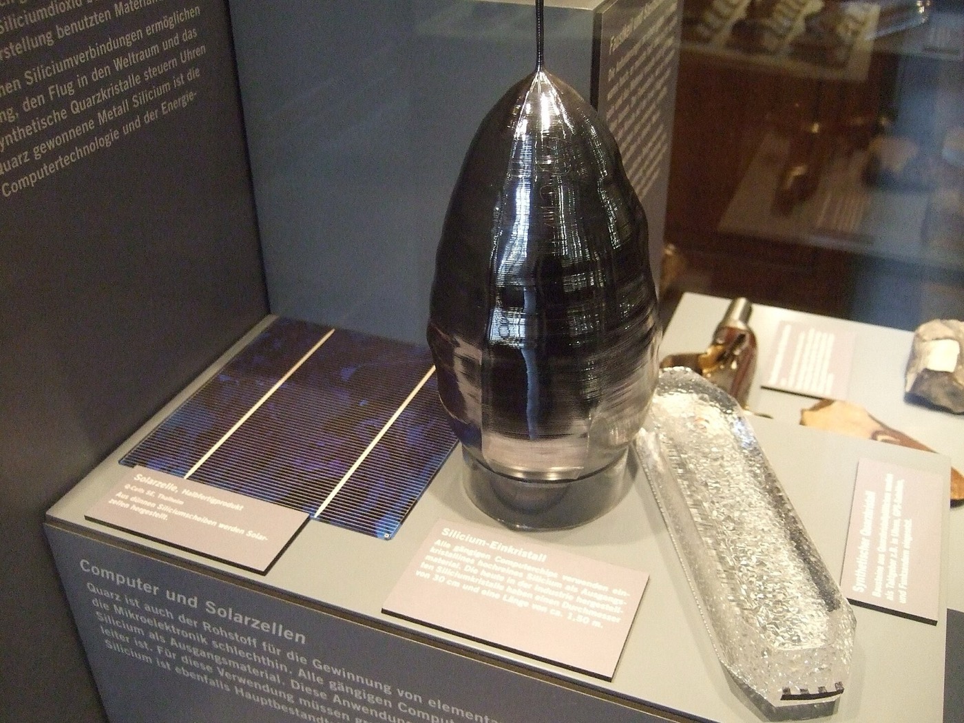
As the seed rises, the silicon freezes onto it as one continuous crystal. Every atom lines up in the same pattern, all the way through. The result is a long cylinder called an ingot, and that regularity is what the switches will depend on.
This is one of those ingots, sometimes called a boule. It is a single crystal of silicon from end to end.
Today the ingot is ground to a standard diameter of three hundred millimetres, about twelve inches. It is sliced into thin discs, and each disc is polished until it shines like a mirror. Those discs are wafers: the wafer is the disc of silicon that many chips are made on at once.
When the work is done, the wafer is cut up, and each piece is called a die. The die is the chip itself, the small square of silicon that ends up inside the package you see on a circuit board. Everything that makes it a chip is printed onto it while it is still part of the wafer.
7. Printing with light
A chip is built up on the wafer in layers, and each layer has its own pattern. According to ASML, the Dutch company whose machines print those patterns, a modern chip can have up to a hundred layers. All of them have to line up on top of each other to within nanometres.
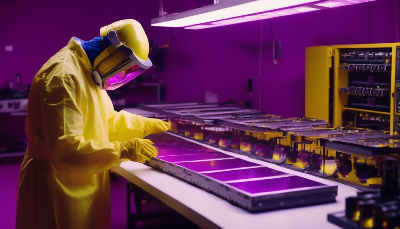
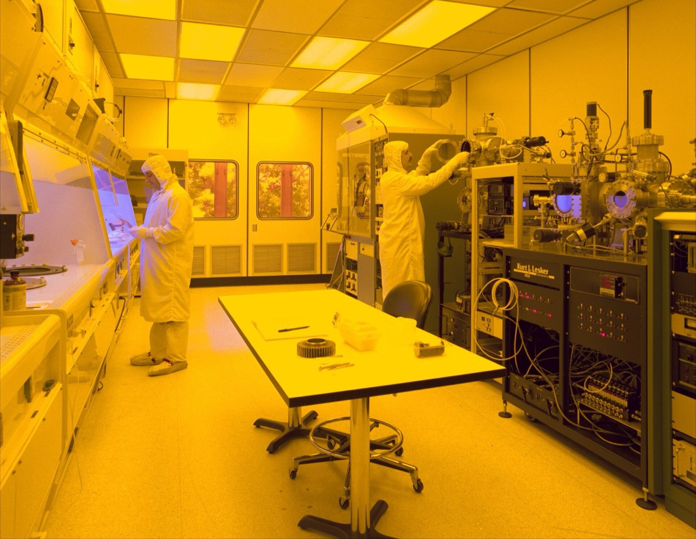
The patterns are printed with light, in rooms like this one. It is a clean room, where the air is filtered to keep out dust, because a single speck can ruin a chip. The yellow light is there because the coating being printed on would react to bluer light.
The technique is called lithography, which means printing the pattern of a circuit onto silicon with light. First the wafer is coated with photoresist, which is the light-sensitive coating that records the pattern. Then light is shone through a mask, a plate carrying the pattern for that one layer.
Each layer goes round the same loop. The exposed coating is developed, rather like a photograph, so the pattern appears. The uncovered material is etched away, or new material is added, and then the leftover coating is stripped off. Then the wafer is coated again, ready for the next layer.
Across all the layers, that adds up to hundreds of steps. ASML says making a chip can take up to four months from design to mass production. And the machines doing the printing are not all the same.
The finest patterns need the shortest light. Most layers are printed with deep ultraviolet light from an argon-fluoride laser, one hundred and ninety-three nanometres in wavelength. The very finest are printed with extreme ultraviolet, which is light with a wavelength of just thirteen point five nanometres.
Why not use extreme ultraviolet for everything? Because it is by far the hardest light to make, and the machine that makes it is the most complicated in the whole industry.
8. EUV, the hardest machine
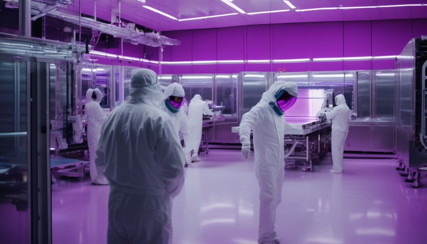
Ordinary lenses cannot handle this light. According to ASML, extreme ultraviolet, or EUV, is absorbed by everything, even air.
So the light is made inside the machine, in a vacuum. A tiny drop of molten tin is fired into a chamber and hit by two laser pulses. The tin turns into a glowing plasma, and that plasma gives off light at thirteen point five nanometres.
The machine does this up to fifty thousand times a second. Mirrors, not lenses, then guide the light, and they shrink the pattern on the mask by a factor of four. Every part of the path, from the source to the wafer, is kept in a high vacuum.
The wafer itself is moving the whole time, to expose one patch after another. ASML says the stage carrying it holds the wafer to within a quarter of a nanometre for each exposure. It checks and adjusts that position twenty thousand times a second.
That is the contrast at the heart of this video. The name on the node went vague just as the machines making it became precise to a fraction of a nanometre.
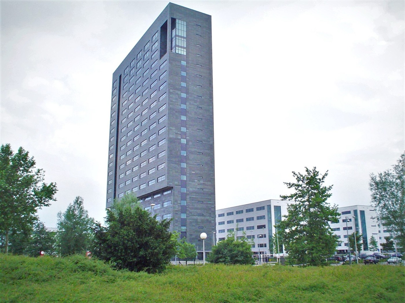
Only one company builds these machines for chipmaking. ASML is based in the Dutch town of Veldhoven, and this is its headquarters. Reuters describes its machines as indispensable to chipmakers such as TSMC, Intel and Samsung.
In December twenty twenty-five, the news agency Reuters reported that only ASML had mastered the technology. It put the price of each machine at about two hundred and fifty million dollars. ASML does not publish its prices, so that figure is the agency's estimate.
The newest version goes further. ASML calls it High-NA, and NA stands for numerical aperture, which is how widely the optics gather light. The standard machines print details down to thirteen nanometres, and the High-NA machines down to eight.
9. Fins, then ribbons
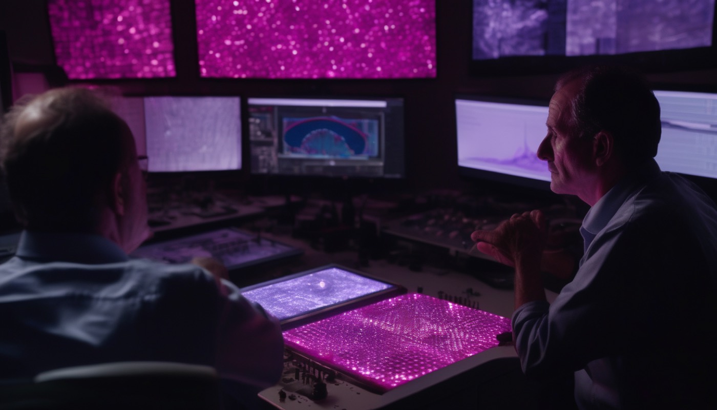
Shrinking the gate had a problem. As the channel under it got shorter, the gate lost its grip, and current began to leak through even when the switch was meant to be off. A switch that leaks wastes power and gets hot.
The answer was to change the transistor's shape. In a flat, or planar, transistor, the gate sits on top of the channel and touches it on one side only. Intel's answer was to stand the channel up as a thin fin, and to wrap the gate over it on three sides.
Intel announced this tri-gate design on the fourth of May, twenty eleven, for its twenty-two nanometre chips. Against its own flat transistors of the generation before, it claimed up to thirty-seven per cent more speed at low voltage. It also said they could use less than half the power at the same performance.
The industry calls this shape a FinFET, which is a transistor with the channel standing up like a fin. It became the standard design at the leading edge for more than a decade. And its real dimensions showed how loose the name had become.
In twenty thirteen, IEEE Spectrum reported the real sizes inside Intel's twenty-two nanometre FinFET. Its fins were just eight nanometres wide, while its gates were longer than twenty-two. Intel's Mark Bohr put it simply: "Some dimensions are smaller than the stated node name, and others are larger."
Fins could only be stretched so far. The next step wraps the gate right round the channel.
This design is called gate-all-around: it is a transistor shape where the control gate wraps the channel on every side. Samsung began production with it on the thirtieth of June, twenty twenty-two, on a node it calls three nanometre. Against its own five nanometre node, it claimed up to forty-five per cent less power.
The others followed. TSMC, the Taiwanese company that makes chips to other companies' designs, began volume production of its N2 node, with nanosheet transistors, in the last quarter of twenty twenty-five. Intel launched its first chips on its own version, at the Consumer Electronics Show in January twenty twenty-six.
Intel calls its version RibbonFET, because the channels are flat ribbons stacked on top of each other. Intel describes it as its first new transistor architecture in more than a decade. The switch had grown upwards and then been wrapped, rather than simply getting smaller.
10. Why the name is not a measurement
By now the name was plainly a label. And the companies themselves said so, in writing.
On the twenty-sixth of July, twenty twenty-one, Intel renamed its manufacturing generations. Its announcement said that "traditional nanometer-based process node naming stopped matching the actual gate-length metric" in nineteen ninety-seven. It added that the industry had long recognised this.
The node Intel had called ten nanometre Enhanced SuperFin became Intel 7. Nothing on the chip got smaller when the name changed. Intel said the node gave ten to fifteen per cent more performance for each watt of power than the ten nanometre version before it.
So if the name is not a length, what does shrink? The two measurements engineers watch most closely are pitches. Gate pitch is the distance from one gate to the next, and metal pitch is the spacing of the finest wires that connect the transistors.
Together they set the transistor density, which is how many switches fit in a given area of silicon. The roadmap scheme IEEE Spectrum reported in twenty twenty names a node by those pitches, plus the number of layers of transistors. That is where the forty-eight and the thirty-six from the start of this video came from.
Paolo Gargini, who proposed the scheme, told the magazine the old node number had absolutely no meaning. It had lost it, he said, because "it had nothing to do with any dimension that you can find on the die". The chipmakers still sell their nodes under their own names.
Instead, the companies publish their progress as ratios against their own earlier nodes. Intel says its eighteen A node gives up to fifteen per cent better performance per watt than Intel three. It also claims thirty per cent better chip density, based on its own internal analysis from February twenty twenty-four.
Notice what is missing from those figures. Neither of them is a size.
Put in order, the story is short. The name stopped matching the gate in nineteen ninety-seven. A proposal to replace it with real pitches was published in twenty twenty. And Intel renamed its own nodes the year after, in twenty twenty-one.
11. The fab and who can build one

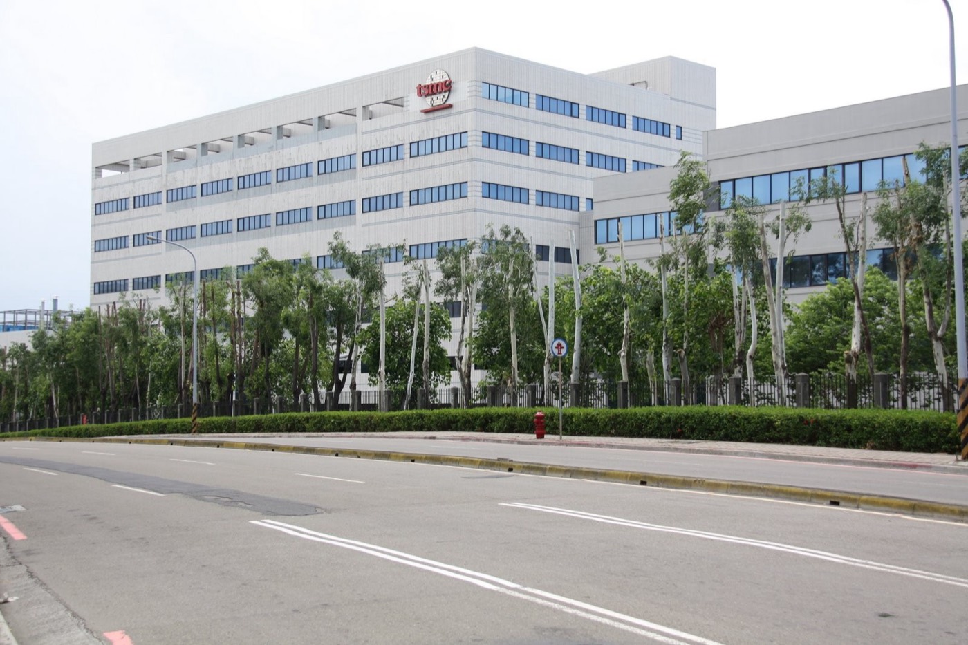

All of this happens in a building called a fab, short for fabrication plant. And building one at the leading edge is now an enormous bet.
The Boston Consulting Group has estimated the cost of a leading-edge fab finishing in twenty twenty-six, making chips at two nanometres and below. Over its first ten years, it put the total cost of owning one at thirty-five to forty-three billion dollars. That covers building it, equipping it and running it.
Very few companies can take that on. Most chip companies design their chips and have them made by a foundry, which is a company that owns the factory and makes chips to other companies' designs.
The best-known foundry is TSMC, short for Taiwan Semiconductor Manufacturing Company. Its home is the Hsinchu Science Park in Taiwan, and this is one of its factory buildings there.
Three companies are racing to make the smallest nodes: TSMC, Samsung and Intel. TSMC's leading factories are mainly in Taiwan, and Samsung's in South Korea. Intel makes its eighteen A chips at a fab in Chandler, Arizona, called Fab fifty-two.
This is one of Samsung's chip campuses, at Pyeongtaek, south of Seoul. The photograph was taken during a visit by the American president.
The factories are also starting to spread out. In March twenty twenty-five, TSMC said it would raise its investment in the United States to one hundred and sixty-five billion dollars. That covers six fabs in Arizona, with two packaging plants and a research centre.
Every one of those buildings is built around the same machines, the same light and the same patient loop of coating, printing and etching. The difference between them is how fine a pattern they can hold.
12. Angstroms and what comes next
The names are now running out of nanometres. The next ones are counted in angstroms, and an angstrom is a tenth of a nanometre.
Intel's eighteen A stands for eighteen angstroms, which is one point eight nanometres. Intel started using angstrom names in twenty twenty-one, in the same announcement that admitted the old names had stopped matching. Like every node name since the late nineteen nineties, it is not a measurement.
TSMC's roadmap has its own angstrom nodes. At its technology symposium in April twenty twenty-six, it moved volume production of A sixteen to twenty twenty-seven. A sixteen is its first node with power delivered from the back of the wafer. After that comes A fourteen. Then A thirteen and A twelve follow in twenty twenty-nine.
The Taiwanese paper Commercial Times, as reported by TrendForce, says TSMC could start pilot production of A fourteen as early as the first quarter of twenty twenty-seven. The financial news service MoneyDJ expects A fourteen to use twenty-five to thirty per cent less power than N2 at the same speed. Neither figure is a size either.
Intel's next node, fourteen A, is planned to use the High-NA machines. In September twenty twenty-six, Intel's finance chief David Zinsner said its defects were falling faster than on any node since twenty-two nanometres. Intel plans risk production in the second half of twenty twenty-seven, and volume production in twenty twenty-eight.
Samsung, meanwhile, says its Exynos 2600 phone chip is the first made on a two nanometre gate-all-around process. It announced the chip in December twenty twenty-five.
Newcomers are trying too. In Japan, Rapidus began making prototype two nanometre transistors in July twenty twenty-five, at its plant in Chitose, on the island of Hokkaido. It aims for mass production in twenty twenty-seven. In China, Reuters reported that a prototype extreme ultraviolet machine was being tested in Shenzhen, with chips from it targeted for twenty twenty-eight.
So what does three nanometres measure? Not the gate, and not the wires. It names a generation: a set of machines, materials and recipes, and a promise that this one packs more in than the last.
If you want to know how far a chip has really moved on, ask different questions. How close together are the gates, and how fine are the wires? How many transistors fit in each square millimetre, and how much power do they use? Those are the numbers the name used to stand for, before nineteen ninety-seven.
The light that prints the finest layers has a wavelength of thirteen point five nanometres, and the newest names are already a tenth of that. The name tells you the generation. It stopped telling you a size a long time ago.
Sources and credits
Photo credits (Wikimedia Commons)
- John Bardeen, William Shockley and Walter Brattain, inventors of the transistor, Bell Labs publicity photo 1948: AT&T; photographer: Jack St. (last part of name not stamped well enough to read), New York, New York., Public domain - https://commons.wikimedia.org/wiki/File%3ABardeen_Shockley_Brattain_1948.JPG
- Replica of the first point-contact transistor, Bell Labs, December 1947: Federal employee, Public domain - https://commons.wikimedia.org/wiki/File%3AReplica-of-first-transistor.jpg
- Bell Telephone Laboratories, Murray Hill, New Jersey, 1942 (Gottscho-Schleisner, Library of Congress): Gottscho-Schleisner Collection, Public domain - https://commons.wikimedia.org/wiki/File%3ABell_Telephone_Laboratory%2C_Murray_Hill%2C_New_Jersey._LOC_gsc.5a08489.jpg
- Intel 4004 chip layout drawing, 1971 (exhibited at VCFB 2016): Wolfgang Stief from Tittmoning, Germany, CC0 - https://commons.wikimedia.org/wiki/File%3AIntel_4004_Chip_Layout_%2829983532570%29.jpg
- Silicon crystal being grown by the Czochralski process, Raytheon plant, Newton MA, 1956: George E. Meyers, Public domain - https://commons.wikimedia.org/wiki/File%3ASilicon_grown_by_Czochralski_process_1956.jpg
- Single-crystal silicon boule (Czochralski ingot), Museum fuer Naturkunde Berlin: Sebastian Wallroth, Public domain - https://commons.wikimedia.org/wiki/File%3ASingle-crystal_silicon_boule.jpg
- Semiconductor clean room under yellow photolithography light (NASA): Uploaded by Duk 08:45, 16 Feb 2005 (UTC), Public domain - https://commons.wikimedia.org/wiki/File%3AClean_room.jpg
- ASML headquarters, Veldhoven, Netherlands, 2008: A ansems, Public domain - https://commons.wikimedia.org/wiki/File%3AASML_headquarters_Veldhoven.jpg
- TSMC factory building, Hsinchu Science Park, Taiwan, 2009: Arusanov, Public domain - https://commons.wikimedia.org/wiki/File%3ATsmc_factory_hsinchu.JPG
- Samsung Electronics Pyeongtaek semiconductor campus, 20 May 2022 (US presidential visit): Office of the President of the United States, Public domain - https://commons.wikimedia.org/wiki/File%3APresident_Biden_visited_the_Samsung_Electronics_Pyeongtaek_Campus_%281%29.jpg


Primary sources
- Computer History Museum, The Silicon Engine timeline and pages (1947 point-contact transistor; 1958 Kilby; 1959 Hoerni planar and Noyce patent; 1965 Moore; 1971 microprocessor; 1974 Dennard) -.
- Intel, 'Intel 4004 processor celebrates 40th anniversary' fact sheet, 2011 - 15 Nov 1971, 2,300 transistors, 10 micron process.
- IEEE Spectrum, Rachel Courtland, 'The Status of Moore's Law: It's Complicated', 28 Oct 2013 - Mark Bohr quote; Intel 22 nm gate 35 nm, fin 8 nm; 0.35 micron node named for its gate length in the mid-1990s.
- EEJournal, Kevin Morris, 'No More Nanometers', 23 Jul 2020 - node name against gate length; quote.
- IEEE Spectrum, Samuel K. Moore, 'A Better Way to Measure Progress in Semiconductors', 21 Jul 2020 - G48M36 for 5 nm; Paolo Gargini quote.
- Intel, 'Intel Accelerates Process and Packaging Innovations', 26 Jul 2021 (SEC 8-K exhibit 99.1) - naming stopped matching gate length in 1997; Intel 7; angstrom era.
- Intel, 'Intel Reinvents Transistors Using New 3-D Structure', 4 May 2011.
- Samsung, 'Samsung Begins Chip Production Using 3nm Process Technology With GAA Architecture', 30 Jun 2022.
- Intel, 'Intel Unveils Panther Lake Architecture', 9 Oct 2025 - 18A vs Intel 3 (Intel internal analysis, Feb 2024); Fab 52, Chandler, Arizona. Intel, CES 2026 release, 5 Jan 2026.
- Reuters, 17 Dec 2025 (as republished) - only ASML has mastered EUV; about $250 million per machine; Chinese prototype in Shenzhen, chips targeted for 2028.
- Rapidus, 'What are the raw materials of semiconductors?', 27 Feb 2026 (eleven nines; Czochralski; 300 mm) and 2 nm GAA prototype release, 18 Jul 2025.
- BCG, 'Navigating the Costly Economics of Chip Making', 28 Sep 2023 - ten-year total cost of ownership $35-43bn for a fab completed in 2026.
- TSMC, 'TSMC Intends to Expand Its Investment in the United States to US$165 Billion', 4 Mar 2025.
- TrendForce, 23 Apr 2026 (TSMC roadmap), 1 Sep 2026 (Intel 14A), 22 Sep 2026 (A14 pilot, citing Commercial Times and MoneyDJ). TechSpot, 19 Dec 2025 (Exynos 2600).
Not regulated financial advice.